Printed Circuit Boards (PCBs) serve as the technological foundation for countless electronic devices, from the humble microwave oven to cutting-edge smartphones. They are the intricate pathways of connectivity, channeling electricity to all the right places within your devices. PCBs, like any complex system, can develop flaws over time.
Everyday use, parts wearing out, or getting too hot can cause these issues. But don’t stress! In this detailed guide, we’ll explore the ins and outs of fixing PCB repair boards, equipping you with the abilities and info you need to tackle this seemingly daunting job. A printed circuit board is another crucial component in modern electronics.
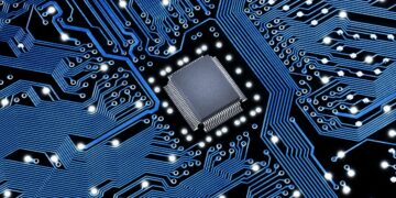
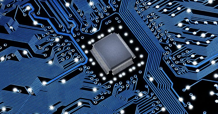
It serves as a platform for connecting and supporting many different electronics in a neat and small way. PCBs are typically made of a non-conductive material, such as plastic or epoxy, with a tiny amount of a conductor, typically copper laminated onto the surface.
Step-by-Step PCB Board Repair Process
Let’s expand on each step in the PCB board repair process.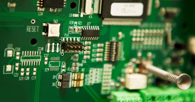
1. Visual Inspection:
- During this phase, carefully scrutinize the PCB for any visible damage. Look for:
- Burnt areas: Blackened or discolored spots, often the result of excessive heat or electrical surges.
- Cracked solder joints: Fractured connections between components and the PCB.
- Damaged components: Any components that appear physically damaged, dislodged, or have visible issues.
- Signs of corrosion: Green or white deposits on the copper traces, usually indicating exposure to moisture.
2. Diagnose Electrically:
- Identify open circuits: Places where electrical continuity is disrupted.
- Detect short circuits: Points where there is unintended and improper connectivity, often caused by solder bridges or damaged traces.
- Measure resistance values to pinpoint any anomalies.
3. Ensure the device is completely powered off and unplugged:
- Safety is paramount. By cutting off power and unplugging the device.
- you eliminate the risk of electrical shocks or damage to the PCB while working on it.
- To further prevent electrical shocks, discharge any capacitors. Capacitors can store electrical energy, even after the device is powered off.
- Use a suitable resistor to discharge them safely.
4. Wear appropriate safety gear:
- Protect your eyes with safety goggles to shield them from potential solder splashes and debris.
- Ensure proper Electrostatic Discharge (ESD) protection, such as wristbands and ESD mats, especially when handling sensitive electronic components.
- ESD can damage or destroy delicate parts.
5. Soldering and Desoldering:
- For cracked or damaged solder joints, use the soldering iron to reheat and melt the solder.
- Allowing it to flow and create a secure connection.
- Apply a fresh layer of solder if needed to ensure a strong bond.
6. Desoldering Components:
- When a component needs replacement, carefully desolder it using the appropriate desoldering tool, like a desoldering pump or wick.
- This will remove excess solder and make component removal easier.
7. Repairing Traces:
- If a copper trace on the PCB is damaged, gently scrape away the damaged section to reveal clean and fresh copper beneath.
- This will prepare the area for repair.
8. Bridge the Gap:
- Use the soldering iron to solder a fine wire, such as a piece of copper wire or a jumper wire, across the damaged trace to bridge the gap.
- Ensure the wire is securely connected on both ends to establish a solid electrical connection.
9. Know Component Specifications:
- Before replacing a component, identify its exact specifications, including its value (e.g., resistance or capacitance), package type, and polarity (if applicable).
- This ensures that the replacement component is compatible.
10. Desolder and Resolder:
- Carefully desolder the faulty component using the desoldering tools.
- Place the new component in its position and solder it in place,
- Paying close attention to its orientation and ensuring secure connections.
11. Multimeter Testing:
- After each repair or component replacement, use the multimeter to test the PCB for proper connectivity.
- Verify that any open circuits are now closed, and short circuits have been resolved.
12. Functional Testing:
- If applicable, power on the device and check that it functions as intended.
- This step confirms that the PCB repair was successful.
13. Inspection:
- Carefully inspect the repaired area to ensure there are no solder bridges (unintended connections) or any other unintended issues.
14. Cleaning:
- Clean the PCB with isopropyl alcohol to remove any flux residue or contaminants left from the soldering and desoldering process.
- This helps maintain the PCB’s cleanliness and functionality.
Common PCB Board Problems:
Before embarking on a journey of PCB board repair, it’s crucial to identify the potential issues you might encounter. Some common problems include.
1. Solder Joint Issues:
- Solder joints are the essential links that secure electronic components to the PCB. These connections are created by melting solder, a metallic alloy, and letting it cool, forming a solid joint.
- Over time, solder joints can experience mechanical stress from thermal expansion and contraction, mechanical vibrations, or even accidental physical impacts. These stressors can lead to solder joints cracking or breaking.
- When solder joints fail, they cause a poor electrical connection. This means that the electrical signals can’t efficiently flow between the component and the PCB, resulting in intermittent or complete loss of functionality.
2. Burned or Damaged Traces:
- Copper traces on a PCB are like the “highways” that guide electrical current to various components. However, they are susceptible to damage from electrical surges, overheating, or physical harm.
- Electrical surges, whether from power supply irregularities or external factors, can cause excess current to flow through the copper traces, overheating and potentially damaging them.
- Excessive heat generated by components can also lead to trace damage. This is why it’s crucial to ensure proper ventilation and cooling in electronic devices.
- Physical damage, like scratches or gouges, can interrupt the copper traces, obstructing the path for electrical current.
3. Component Failures:
- Component failures can also result from misuse or abuse. For instance, applying voltage beyond the specified limit, dropping the device, or subjecting it to harsh environmental conditions can lead to the premature failure of components.
- When a component fails, it can cause a domino effect, affecting the performance of the entire PCB and the device it powers.
4. Corrosion:
- Corrosion is a gradual and often invisible enemy of PCBs, especially in humid or corrosive environments. It occurs when moisture, oxygen, and other contaminants come into contact with the metal components of the PCB, particularly copper.
- Corrosion can weaken or corrode the copper traces, leading to poor connectivity and increased resistance.
- It’s essential to protect PCBs in humid or corrosive environments through the use of conformal coatings, which shield the components from moisture and contaminants.
Conclusion
Repairing a Printed Circuit Board (PCB) is an empowering skill that can breathe new life into your beloved electronic devices. This guide has walked you through the detailed process, highlighting the importance of precision, care, and safety at each step of PCB board repair. By visually and electrically identifying problems, preparing your workspace for safety, mastering soldering and desoldering techniques, repairing traces, and replacing components with precision, you’re well on your way to becoming a PCB board repair enthusiast.
Comprehensive testing, both with a multimeter and functional testing, ensures the success of your repairs, while a final touch of cleanliness and inspection keeps your PCB in top shape. Remember, with practice and patience, you can extend the life of your devices and make a positive contribution to a more sustainable future.


